What is SEMICON Japan? | International Exhibition for Semiconductor Manufacturing Equipment, Materials, Advanced Packaging, Inspection & Metrology
What is SEMICON Japan?
SEMICON Japan is an international exhibition covering the semiconductor and microelectronics industry supply chain, including semiconductor manufacturing equipment, materials, parts and components, inspection and metrology, advanced packaging, semiconductor design and manufacturing automation.
Organized by SEMI, the exhibition brings together semiconductor manufacturers, manufacturing equipment suppliers, materials manufacturers, technology companies and research institutions from Japan and overseas to present the latest technologies.
Launched in Harumi, Tokyo in 1977, SEMICON Japan will celebrate its 50th edition in 2026. While semiconductor manufacturing technology remains at its core, the exhibition has expanded to cover advanced application fields such as AI, data centers, automotive, IoT, healthcare, robotics and GX.
One of its key features is the ability to compare a broad range of technologies across the semiconductor manufacturing process, from equipment and materials to advanced packaging, inspection and metrology, manufacturing data utilization and supply-chain solutions.
Event Overview
| Exhibition | SEMICON Japan 2026 – 50th Edition |
|---|---|
| English Name | SEMICON Japan 2026 |
| Theme | Semiconductors: The Past 50 Years and the Next 50 Years |
| Dates | December 9, 2026 (Wednesday) – December 11, 2026 (Friday) |
| Hours | 10:00–17:00 |
| Venues | Tokyo Big Sight, Ariake Central Tower Hall & Conference, and TFT Building |
| Tokyo Big Sight Exhibition Areas | East Exhibition Halls 4–6, West and South Exhibition Halls, Conference Tower and other areas, based on organizer information |
| Address | 3-11-1 Ariake, Koto-ku, Tokyo, Japan (Tokyo Big Sight) |
| Organizer | SEMI |
| Admission | Free with advance registration. Visitors are required to print their admission badge. |
| Concurrent Events | Advanced Packaging and Chiplet Summit (APCS), Advanced Design Innovation Summit (ADIS), Metrology & Inspection Summit (MIS) |
| Official Website | https://www.semiconjapan.org/jp |
As the venue configuration has changed for 2026, visitors should check the official floor map before attending to confirm the location of their target exhibition areas.
Main Exhibition Categories
Semiconductor Manufacturing Equipment
This category covers equipment and technologies for semiconductor front-end processes, including lithography, deposition, etching, cleaning, thermal processing, ion implantation and CMP.
Technologies supporting device scaling, higher performance, yield improvement, productivity enhancement and energy efficiency are presented.
Semiconductor Materials & Electronic Materials
This category includes silicon wafers, photoresists, specialty gases, process chemicals, target materials, insulating materials, encapsulation materials and other materials used in semiconductor manufacturing and packaging.
Inspection, Metrology & Quality Control
Defect inspection systems, dimensional metrology, film-thickness measurement, wafer inspection, visual inspection and testing equipment supporting manufacturing quality and yield improvement are presented.
Advanced Packaging & Chiplets
This category covers technologies supporting higher semiconductor performance and high-density integration, including advanced packaging, 2.5D and 3D integration, chiplets, bonding, substrates, encapsulation and thermal management.
Semiconductor Design & Verification
Technologies supporting next-generation semiconductor design and development are presented, including EDA, design automation, simulation, design verification and semiconductor IP.
Manufacturing Equipment Parts & Components
This category includes vacuum equipment, pumps, valves, flow-control systems, temperature-control equipment, precision components and material-handling systems used in semiconductor manufacturing equipment.
Cleanrooms & Factory Infrastructure
Technologies supporting stable semiconductor fab operations are presented, including cleanrooms, HVAC and environmental control, ultrapure water systems, gas supply, exhaust treatment and chemical supply systems.
Smart Factory & Manufacturing DX
This category covers technologies that improve semiconductor fab productivity and quality, including manufacturing data collection and analysis, equipment monitoring, predictive maintenance, automated material handling and AI-based process optimization.
Back-End Processes, Assembly & Testing
Equipment and technologies for semiconductor back-end processes are presented, including dicing, bonding, encapsulation, packaging, testing and inspection.
Environment & Sustainability
This category covers technologies for reducing the environmental impact of semiconductor manufacturing, including greenhouse-gas reduction, energy efficiency, water-resource management, chemical management and resource circulation.
Semiconductor Supply Chain & Related Services
Services supporting the semiconductor industry supply chain are presented, including materials procurement, contract manufacturing, logistics, equipment maintenance, technical support and workforce development.
Concurrent Summits
Advanced Packaging and Chiplet Summit (APCS)
This summit focuses on advanced packaging, chiplets and substrate integration, presenting technologies and industry trends supporting higher semiconductor performance and greater integration density.
Advanced Design Innovation Summit (ADIS)
Exhibitions and presentations focus on next-generation semiconductor design, design verification and development technologies.
Metrology & Inspection Summit (MIS)
This summit focuses on inspection and metrology technologies related to semiconductor manufacturing quality control, advanced process scaling and yield improvement.
Key Features of SEMICON Japan
Coverage of the Semiconductor Manufacturing Supply Chain
Visitors can compare a broad range of technologies involved in semiconductor manufacturing, including manufacturing equipment, materials, components, inspection and metrology, back-end processes and advanced packaging.
Participation by Major Companies and Research Institutions from Japan and Overseas
Semiconductor manufacturers, manufacturing equipment and materials suppliers, research institutions and other organizations gather to create opportunities for technical exchange, business meetings and new customer development.
Business, Technology and Market Intelligence
Keynote presentations, technical symposiums and other programs provide information on semiconductor market trends, advanced technologies, business strategies and workforce development.
Connections with Advanced Application Industries
The exhibition creates opportunities for collaboration with a wide range of semiconductor application industries, including AI, data centers, automotive, IoT, healthcare and robotics.
Supply-Chain Resilience and Sustainability
Important semiconductor industry issues are also addressed, including economic security, supply-chain restructuring, environmental impact reduction and workforce development.
Exhibition Scale
SEMICON Japan 2026 is expected to feature more than 1,200 exhibiting companies and organizations covering the full range of semiconductor manufacturing processes.
This is the planned scale announced by the organizer before the event and does not represent final results confirmed after the 2026 exhibition.
Main Visitor Profiles
- Semiconductor device manufacturers
- Semiconductor manufacturing equipment manufacturers
- Semiconductor and electronic materials manufacturers
- Equipment parts and component manufacturers
- Semiconductor back-end process and packaging companies
- Inspection and metrology equipment manufacturers
- Semiconductor design and EDA companies
- Electronic component and electronics companies
- Automotive and automotive semiconductor companies
- AI and data center companies
- Manufacturing DX and smart factory companies
- R&D and product design professionals
- Production engineering, manufacturing and quality-control professionals
- Equipment investment and procurement professionals
- Executives, business development and investment professionals
- Universities, research institutions and educational organizations
Key Trends in the Semiconductor Industry
Advanced Semiconductors for AI & Data Centers
As generative AI and high-performance computing expand, semiconductor computing performance, power efficiency, memory bandwidth and advanced packaging are becoming increasingly important.
Advanced Packaging & Chiplets
Technologies for densely integrating multiple semiconductor dies and chiplet architectures combining different functions are receiving increasing attention.
More Advanced and Complex Manufacturing Processes
As semiconductor performance increases, technical requirements for advanced patterning, deposition, etching, inspection and metrology are becoming more demanding.
Restructuring of the Semiconductor Supply Chain
From the perspectives of economic security and stable supply, the development of semiconductor manufacturing capacity, diversification of procurement sources and collaboration among companies in Japan and overseas are becoming increasingly important.
Smart Factories & Manufacturing Data Utilization
Initiatives to improve productivity and yield are advancing through manufacturing equipment data collection, AI-based process optimization, predictive maintenance and automated material handling.
Environmental Impact Reduction & GX
Technologies are required to improve management of electricity, water, chemicals and greenhouse gases used in semiconductor manufacturing while reducing environmental impact.
Semiconductor Workforce Development
Developing skilled professionals in manufacturing equipment, materials, design, inspection and metrology is increasingly important, driving interest in industry-academia collaboration and educational programs.
FAQ
What kind of exhibition is SEMICON Japan?
SEMICON Japan is an international exhibition covering the semiconductor and microelectronics supply chain, including semiconductor manufacturing equipment, materials, inspection and metrology, advanced packaging, semiconductor design and manufacturing automation.
What types of companies can exhibit?
Exhibitors include semiconductor manufacturing equipment manufacturers, materials suppliers, parts and component manufacturers, inspection and metrology companies, semiconductor design and back-end process companies, and companies involved in factory infrastructure and manufacturing DX.
Can companies outside semiconductor manufacturing attend?
Yes. The exhibition also targets companies, engineers and researchers from related industries such as semiconductor manufacturing equipment, materials, electronic components, automotive, AI, IoT and medical devices.
Is advance registration required?
Admission is free, but advance registration is required. Visitors should register through the official website and print their admission badge.
When will the next SEMICON Japan be held?
SEMICON Japan 2026 will be held from December 9 to 11, 2026 at Tokyo Big Sight and other venues.
Watch Exhibitor Videos
The videos shown below are randomly selected from this exhibition. To browse all videos from this exhibition, please see the “Featured Exhibitions by Year” section below.
[SEMICON Japan 2022] High Current Connectors/High Temperature Heat Resistant Connectors - Globe Tech Co., Ltd.
[SEMICON Japan 2022] Xradia Versa / Crossbeam - Carl Zeiss Corporation
[SEMICON Japan 2022] Flow Measurement Manifold - Toflo Corporation
[SEMICON Japan 2022] Vacuum Plane Heating Unit - Himeji Rika Co., Ltd.
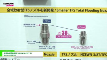
[SEMICON Japan 2022] CABINEX-EWT II FOR SEMICONDUCTOR MANUFACTURING EQUIPMENT - Hatsuda Manufacturing Co., Ltd.
[SEMICON Japan 2022] KUMADE-FORK (EC type) - Hermotech Co., Ltd.
[SEMICON Japan 2022] Probe Card - SEIKEN Co., Ltd.
[SEMICON Japan 2022] Silicon carbide screw - Nabeya Vitec Company
[SEMICON Japan 2022] Raident Processing - Raident Industry Co., Ltd.
Featured Exhibitions by Year
SEMICON Japan 2022 (Japan)
Benefits of Exhibiting
SEMICON Japan is an international exhibition where companies can directly present semiconductor manufacturing equipment, materials, components, inspection and metrology systems, advanced packaging technologies, manufacturing automation solutions and related products and technologies to semiconductor industry professionals from Japan and overseas.
Exhibitors have opportunities to meet R&D, production engineering, equipment investment and procurement professionals from semiconductor device manufacturers, manufacturing equipment suppliers, materials manufacturers, research institutions and other organizations.
Technical advantages and implementation benefits in manufacturing processes can be explained in detail using physical samples, equipment demonstrations, measurement data and product videos.
The exhibition can also be used to develop new customers in Japan and overseas, identify joint-development partners, strengthen relationships with distributors and enter new semiconductor supply chains.
Key Preparation Points for Exhibitors
Before exhibiting, clearly define the target companies and departments you want to prioritize, such as semiconductor device manufacturers, manufacturing equipment suppliers and materials manufacturers.
For semiconductor manufacturing equipment, organize information on processing capacity, supported processes, accuracy, throughput, equipment dimensions, required utilities and maintenance support.
For semiconductor materials, prepare documentation explaining purity, physical properties, heat resistance, chemical resistance, supply capacity and quality-control systems.
For inspection and metrology equipment, present information on measurement principles, detection limits, accuracy, repeatability, processing speed and application examples.
For advanced packaging technologies, organize technical information such as bonding accuracy, packaging density, thermal characteristics and reliability evaluation.
For manufacturing DX products, be prepared to explain integration with existing equipment, methods of using manufacturing data, implementation benefits and security.
If business discussions with overseas companies are expected, prepare English-language product catalogs, technical materials and product videos with subtitles.
Estimated Exhibiting Costs
Booth Fees
Exhibiting fees may vary depending on the number of booths, exhibition area, participation category, application timing and SEMI membership status.
When displaying actual semiconductor manufacturing equipment or inspection and metrology systems, check additional costs related to electrical power, compressed air, exhaust systems and heavy-equipment handling.
Refer to the organizer’s latest exhibitor information for current booth fees and application conditions.
Booth Decoration & Construction Costs
As a general planning estimate, booth construction may cost approximately JPY 300,000–800,000 for one booth, JPY 700,000–1,500,000 for two booths, and JPY 1,500,000 or more for four booths or more.
These are general estimates for exhibition booth construction and are not official construction rates provided by the SEMICON Japan organizer. Booth fees and specialized facility work are not included.
Displays involving large manufacturing equipment, precision measurement systems or clean environments may require additional costs for special electrical systems, heavy-load handling, air conditioning, exhaust systems and safety equipment.
When requesting a quotation from a booth contractor, provide the dimensions and weight of exhibits, required utilities, whether demonstrations will be conducted and the amount of meeting space required.
Personnel Costs
In addition to sales staff, assign technical sales and R&D personnel who can explain semiconductor manufacturing processes, equipment performance, material characteristics, inspection and metrology technologies and related technical details.
Having personnel capable of answering detailed technical questions can lead to concrete discussions about equipment evaluation, material adoption and joint development.
To support meetings with overseas companies, consider assigning personnel who can communicate in English or other foreign languages.
Transportation & Logistics Costs
Budget for transportation, move-in and move-out, packing, insurance, installation and removal of manufacturing equipment, precision measurement systems, semiconductor materials and booth fixtures.
For precision equipment, consider vibration and shock protection. For large equipment, check move-in routes, floor load capacity, material-handling equipment and installation procedures.
If chemicals, specialty gases or other regulated materials will be displayed or used, confirm the organizer’s and venue’s rules and safety requirements in advance.
Contact the exhibition organizer for exact costs.
Booth Examples by Size
1-Booth Exhibit
Suitable for presenting semiconductor materials, precision components, equipment components, compact measurement systems, software and technical services.
Combine product samples, performance-comparison data, technical information panels and monitors so that visitors can understand the technical characteristics in a short time.
2-Booth Exhibit
A possible configuration combines a live display of compact equipment with comparative displays of components and materials and a technical consultation area.
Use measurement data and manufacturing-process videos to clearly communicate the benefits of adopting the equipment or materials.
4 Booths or More
Suitable for companies presenting multiple semiconductor manufacturing systems or related technologies.
The booth can combine live equipment demonstrations, product-category displays, technical presentations and business meeting areas.
When exhibiting large equipment or precision instruments, the design should account for electrical power, exhaust systems, safety equipment and visitor flow.
When selecting a booth contractor, check its experience with semiconductor and electronics exhibitions, track record in handling precision equipment, and photographs or portfolios of previous projects.
Key Elements of a Successful Exhibition Booth
Visitor Flow Design
Separate the flow of visitors watching equipment demonstrations, engineers examining product samples and professionals seeking detailed business discussions.
For large equipment displays, provide a safe viewing area and establish restricted-access zones when necessary.
If equipment evaluation or joint-development consultations are a priority, design a natural route from the product display area to technical meeting spaces.
Visibility
Ensure that the brand name, technology field and problems solved by the product can be clearly identified from the aisle.
Communicate technical benefits concisely, such as “yield improvement,” “support for advanced process scaling,” “high-precision measurement,” “energy saving” and “higher equipment utilization.”
Displaying performance comparison graphs, measurement data and implementation examples helps visitors quickly assess the relevance of the solution to their own challenges.
Demonstration & Experience Design
For semiconductor manufacturing equipment, live demonstrations and videos explaining operating principles, process flows and performance comparisons are effective.
For inspection and metrology equipment, demonstrating actual measurement procedures and data visualization helps communicate the equipment’s characteristics more clearly.
For materials, explain technical advantages using data on physical properties, purity, heat resistance and reliability evaluation.
During demonstrations, consider electrical power, high-temperature areas, moving parts, chemicals, gases and visitor safety.
Using Video at the Exhibition
Showing product introduction videos of approximately 2–3 minutes on monitors or LED displays in the booth can efficiently explain processes such as deposition, etching, cleaning, inspection and metrology, and packaging.
Video is particularly effective for showing content that is difficult to reproduce at the exhibition venue, such as actual semiconductor fab operations, internal equipment structures, manufacturing processes and changes in measurement data.
If the content is intended for semiconductor manufacturers and R&D professionals overseas, consider multilingual support such as English subtitles.
Looping videos allows product information to continue reaching visitors even while staff members are engaged in technical consultations or business meetings.
Product explanations by company representatives or technical staff can also be recorded at the exhibition and edited into approximately 2–3 minute videos for distribution on the same day or the following day.
Completed videos can be reused on the company’s website, YouTube, social media, sales emails, product pages and materials for overseas distributors.
By continuing to publish them on Internet Exhibition.tv, product information can also reach R&D, production engineering and manufacturing professionals in Japan and overseas who were unable to attend the exhibition.
Videos introducing semiconductor manufacturing equipment and materials technologies can become long-term assets for sales activities and technical communication even after the exhibition ends.
If a booth contractor can provide both booth construction and video production, equipment placement, lighting, monitors, LED displays, safety equipment and filming positions can be planned together from the design stage.
Strategies for Attracting Visitors and Improving Exhibition Results
Email Marketing
Send exhibition announcements to R&D, production engineering and procurement professionals at semiconductor device manufacturers, manufacturing equipment suppliers and materials manufacturers, as well as existing customers and companies considering equipment investments.
Introduce the products to be exhibited, technical features, planned equipment demonstrations and booth number to encourage advance meeting reservations.
Social Media
Use LinkedIn, YouTube and other platforms to publish videos of manufacturing equipment in operation, technical explanations, measurement data and implementation examples.
Short videos explaining the technical advantages of products can increase interest among R&D and production engineering professionals in Japan and overseas.
Invitations & Direct Mail
Send individual invitations and technical materials to R&D, equipment investment and procurement departments of semiconductor manufacturers and manufacturing equipment suppliers that you want to prioritize.
Announce equipment demonstration and technical consultation schedules in advance to encourage concrete business meeting reservations.
Exhibition Landing Page
Create a dedicated exhibition Landing Page featuring exhibited products, booth number, technical specifications, implementation examples, product videos, catalogs and a technical consultation reservation form.
After the exhibition, the page can continue to serve as an information resource for companies considering equipment investment, material adoption or joint development.
Companies Available for Booth Construction and Exhibition Operations Consultation
When exhibiting at SEMICON Japan, it is important to select a booth contractor capable of handling technical exhibits involving semiconductor manufacturing equipment, precision instruments and electronic materials.
Check whether the contractor can support the move-in and installation of large equipment, handling of precision instruments, electrical work, equipment demonstration areas, safety equipment, lighting, monitors and LED displays according to the exhibition requirements.
Product demonstrations and explanations by technical personnel can also be filmed at the exhibition and edited into videos of approximately 2–3 minutes on the same day or the following day, enabling timely communication during the event.
By continuing to publish completed videos not only on the company’s website and social media but also on Internet Exhibition.tv, product information can continue reaching R&D, production engineering and manufacturing professionals in Japan and overseas even after the exhibition ends.
Please see the booth construction company pages below.
SPORTEC Booth Design & Construction Companies
Request a Booth Contractor Recommendation and Receive a Free Exhibitor Video Package
Submit your requirements and our team will recommend suitable contractors.
Looking for a booth design and construction company for this exhibition?
Tell us about your project and requirements.
Our team will review your request and introduce suitable contractors.
As a special benefit, exhibitors who request quotations through our service will receive a complimentary exhibitor video production package.
Your request is not automatically sent to all contractors. We carefully review your requirements and connect you with the most suitable companies.